Infrared sensor is grown directly on its readout chip
Researchers fabricated lead-sulfide detectors directly on the electronics that read them. A 640 × 512-pixel prototype captured infrared images without separately bonding the detector layer.
·4 min read
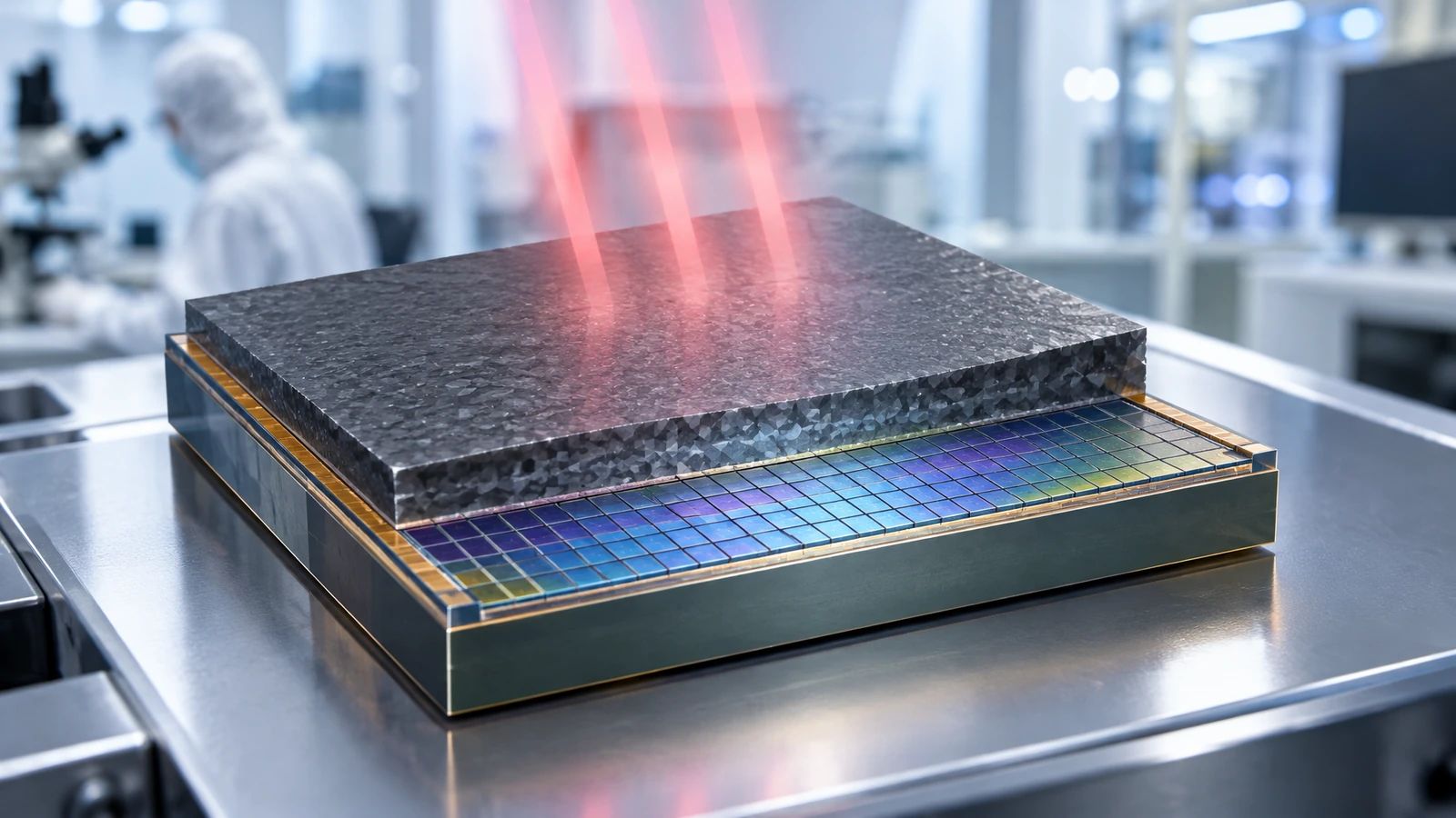
Illustration of monolithic integration of PbS detectors on a readout chip. Not the researchers' actual imaging chip.Illustration generated with OpenAI for Progress Radar
Skipping a separate manufacturing step
Infrared cameras typically combine a detector layer that senses radiation with a separate readout chip that processes signals from the pixels. The two components then have to be connected, adding complexity to manufacturing.
In a peer-reviewed Nature study, researchers demonstrate a different route. They grew the infrared semiconductor lead sulfide, PbS, directly on a finished readout integrated circuit, or ROIC. The method is called monolithic in situ integration, abbreviated MISI.
Instead of high-temperature growth, the process uses an aqueous solution at room temperature. The researchers regulated the chemistry around the lead ions and reduced disturbances during crystallization, allowing PbS to form highly ordered films directly on the electronics underneath.
From solution to an infrared camera
The films were quasi-single-crystalline and showed uniform properties across both wafer and pixel scales. The researchers measured a carrier density of approximately 2 × 10^15 per cubic centimetre and mobility of 124 square centimetres per volt-second.
By doping the PbS material with antimony, the team made photodiodes with a specific detectivity of 4.4 × 10^11 Jones at a wavelength of 2.5 micrometres. In the study, this exceeds the performance the researchers cite for commercial InGaAs detectors at the same wavelength.
That does not mean the PbS camera is better than existing InGaAs cameras in every respect. Detectivity is one performance metric, while complete camera systems must also be judged on factors including noise, speed, stability, manufacturing yield and cost.
640 × 512 pixels
The researchers did not stop at individual photodiodes. They built a 640 × 512-pixel focal-plane array and used it to capture clear infrared images. This demonstrates that the growth method can operate across a full imaging array rather than only in small test structures.
The team also grew the detectors directly on flexible readout circuits, showing that the approach is not necessarily restricted to a flat, rigid sensor platform.
A central advantage of the concept is the integration itself. If the detector layer can be fabricated directly on the readout circuit, the bonding step between two separately manufactured components could in principle be avoided. The researchers therefore describe the method as a possible route toward more scalable manufacturing of advanced optoelectronic sensors.
A promising manufacturing route, not mass production yet
The study demonstrates a working infrared imaging array, but it does not demonstrate a commercial mass-production line. Room-temperature processing directly on existing electronics makes the method interesting for further scaling, while manufacturing yield, long-term stability and cost still need to be evaluated at industrial scale.
The material choice also carries a practical limitation: PbS contains lead. Any large-scale deployment would therefore need appropriate material and waste handling.
The result is primarily a new answer to a manufacturing problem. Instead of producing the detector and readout circuit separately and then trying to connect them perfectly, the researchers show that the detector material itself can grow on the electronics that will read it. That could open a different manufacturing route for infrared cameras if the method can make the transition from laboratory demonstrations to industrial production.
Researchers stretching two slightly rotated, atom-thin graphene sheets measured an electrical response more than a hundred times as sensitive as in ordinary metals, adding a new way to probe quantum materials.
RIKEN researchers built an optical helix by rotating and stacking ultrathin polymer films. Layer orientation, spacing and doping tune the response from visible to near-infrared light.
A new study uses an integrating sphere to turn irregular light patterns into exceptionally precise spectral measurements, reporting roughly 80-fold better resolution than earlier speckle spectrometers.